Bench Degree·PLASMAchapter
Chapter 10: How Every Chip Is Made
There is a dark gap between the glow and the cathode in your jar, and you can measure it with a ruler. That gap, scaled down and aimed at a silicon wafer, is how every transistor in every device you own was given its shape, and there is no other way to do it.
Strike the discharge in the jar at a few Torr and look closely at the negative electrode.
The glow does not touch it. There is a dark space between the metal and the light, and if you pump down further the dark space grows. Let the pressure up and it shrinks.
That dark space is a sheath, and it is the same object Chapter 2 described when a plasma wrapped a stray charge in a coat of opposite charge. Here the stray object is your electrode, and the coat has become a layer with almost the entire voltage of the discharge across it.
Everything a plasma does to a solid, it does through a sheath. The blackened ends of an old fluorescent tube, the eroded wall of an ion thruster, the reading on a probe, and the trench that makes a transistor.
ON THE BENCH: Measure the sheath
Parts: the jar, hand pump, current-limited supply and ballast resistor. A steel rule. A phone camera. Graph paper. Cost: nothing beyond Chapter 6. Time: an hour. Hazards: high voltage, Chapter 16 in full, ballast not optional, and do not touch the jar while it is energised. Method: at each of six or eight pressures, photograph the discharge square on with a rule laid alongside the glass, then measure the dark space in front of the cathode from the photograph. Plot dark space against pressure. What you should see: a few millimetres at a few Torr, growing to 20 mm (0.8 in) or more as you approach the lowest pressure your pump reaches. The product of the two is roughly constant, which will look familiar, because it is Chapter 5’s pressure times distance appearing again for the same reason: what matters is how many collisions an electron makes crossing the gap, not the pressure or the distance alone. If it does not work: a discharge that fills the whole tube with no visible structure is running at too high a current. Increase the ballast resistance and look again.
Section 1: The Problem That Only a Field Can Solve
A pattern is printed in a light-sensitive coating on a layer of silicon or metal or insulator. Where the coating remains, the layer beneath must survive. Where it has been washed away, the layer beneath must be removed, straight down, with vertical walls. The obvious way is acid, and the industry used it for years.
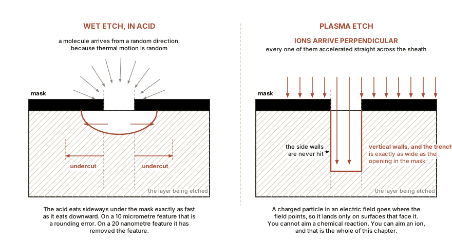
And it fails, because a liquid attacks in every direction at once. Acid removes material downward and sideways at the same rate, so it eats under the edge of the mask, leaving a rounded pit wider at the top than the mask that made it.
If your feature is 10 µm (0.0004 in) across, an undercut of half a micrometre is a rounding error. If your feature is 20 nm across, that undercut has removed the feature entirely.
So the requirement is a process that removes material in one direction and not the others. That property is called anisotropy, and it is the one thing the semiconductor industry needed and could not get from chemistry.
Chemistry is isotropic. A molecule arrives from a random direction because thermal motion is random. You cannot aim a chemical reaction.
But you can aim a charged particle, because a charged particle in an electric field goes where the field points. That is the entire idea of this chapter.
IN PLAIN ENGLISH: Etching with acid is like cleaning a wall with a wet sponge: it works, and it goes everywhere. Etching with a plasma is like cleaning it with a sandblaster held square to the surface. The grit only hits what faces it, and the vertical sides of a groove never get hit. And in a chip factory the grit is chemically reactive too, so it dissolves what it lands on and leaves as a gas.
Section 2: Why the Sheath Points the Ions Down
Put any solid surface into a plasma and leave it floating. Electrons and ions both strike it, but electrons are far lighter and therefore far faster, so many more of them arrive per second. The surface accumulates negative charge.
It keeps accumulating until it is negative enough to repel most of the arriving electrons, at which point arrivals balance and the charging stops. The surface now sits at a voltage below the plasma around it, and a thin region next to it holds that entire voltage difference. That is the sheath, a few Debye lengths thick.
Inside the sheath, the field points from the plasma toward the surface. A positive ion reaching the sheath edge is grabbed and accelerated straight into the surface, arriving perpendicular to it with an energy set by the sheath voltage. That is anisotropy, delivered free by a plasma’s tendency to insulate itself from whatever it touches.
A floating surface only develops a few times the electron temperature, which is tens of volts. The industry wants hundreds, so it drives the wafer electrode deliberately, and the way it does so explains the one number every etch tool shares.
Etch tools run at 13.56 MHz. Two reasons. A wafer being etched is often an insulator, and a direct-current bias cannot be maintained across an insulator because charge piles up, while an alternating field passes through as displacement current. And at that frequency the light electrons can follow the field back and forth within a cycle and the heavy ions cannot, so electrons are swept off the powered electrode on each positive half-cycle and cannot all return. The electrode charges itself negative and stays there, developing a steady self-bias of a few hundred volts under the radio-frequency swing, and the sluggish ions simply fall through that average. The frequency itself is not physics: 13.56 MHz is an internationally allocated industrial band, so a factory full of kilowatt generators does not interfere with anybody’s communications.
Section 3: Reactive Ion Etching, Which Is Two Jobs at Once
Pure bombardment works. Fire argon ions at a surface hard enough and atoms are knocked off mechanically, which is sputtering. It is perfectly anisotropic and nearly useless alone, because it removes everything at about the same rate, including the mask.
Reactive ion etching splits the job in two, and that is the idea that made modern chips possible.
The radicals do the chemistry. A plasma made from a fluorine-bearing gas such as sulphur hexafluoride is full of neutral fluorine atoms, chemically ferocious and electrically neutral, arriving from all directions. Fluorine attacks silicon and turns it into silicon tetrafluoride, which is a gas at room temperature and simply leaves.
The ions do the aiming. Ion bombardment on the horizontal surfaces at the bottom of the trench breaks bonds and clears reaction products, so the chemistry proceeds far faster there than on the vertical walls, which no ion ever strikes.
Three working rules follow:
The product must be volatile, and that dictates the gas. Fluorine for silicon, because silicon tetrafluoride is a gas. Chlorine for aluminium, because aluminium chloride is volatile and aluminium fluoride is not, so a fluorine plasma would coat an aluminium wafer in a crust and stop. You do not choose the etch gas by what attacks the material. You choose it by what carries the material away.
Selectivity is engineered with a polymer. Add a carbon-rich gas and the plasma deposits a thin film everywhere. Bombardment strips it from the trench bottom and cannot reach the walls, so the walls stay coated and protected while the bottom keeps etching.
And for deep features the two steps are alternated, hundreds of times, which is the Bosch process and is how the deep holes in pressure sensors and stacked memory are made. A hole in a modern stacked flash memory is roughly 100 nm across and 6 µm (0.00024 in) deep, sixty times deeper than it is wide, several billion of them at once.
SLOW DOWN. Check Your Understanding: Etch tools run at 1 to 100 mTorr, a hundred to ten thousand times lower pressure than your jar. Lower pressure means a weaker glow and a slower reaction, so it costs throughput. Why pay that, and why does going lower make the walls straighter? Answer before reading on.
Because of what happens to an ion while it crosses the sheath. The field accelerates it straight at the wafer, and if it arrives without hitting anything it arrives perpendicular. If it collides with a neutral molecule on the way it is deflected, and an ion arriving at an angle hits a sidewall.
So the ion’s mean free path must be longer than the sheath is thick. At 10 mTorr the mean free path is about 6 mm (0.24 in) and the sheath is a millimetre or two, so most ions cross without a single collision. At 100 mTorr the mean free path falls to about 0.6 mm (0.024 in), shorter than the sheath, so nearly every ion is scattered and the directionality is lost.
Now run the same arithmetic on your own jar. At 5 Torr the mean free path is about 12 µm (0.0005 in), a thousandth of the dark space you measured. Every ion reaching your cathode has been scattered hundreds of times. Your jar cannot etch anisotropically, and that is the number which says why, rather than a vague appeal to laboratory equipment.
Section 4: The Other Half, Which Is Putting Material On
A chip is fifty to a hundred stacked layers, so something has to put them there, and plasma does that too.
Plasma-enhanced chemical vapour deposition. Flow a gas over a hot wafer and it decomposes, leaving a solid film. Silicon nitride from silane and ammonia is the classic, and done thermally it needs about 800 °C (1,472 °F).
Which is impossible, because by the time insulators are being laid between metal layers there is aluminium on the wafer, and aluminium melts at 660 °C (1,220 °F). Worse, everything built earlier cooks again every time you heat it, and dopants diffuse.
Strike a plasma in the same gas and the energetic electrons break the molecules apart for you. The energy for the reaction now comes from the field rather than from the wafer’s temperature, so the same film deposits at 300 to 400 °C (572 to 752 °F). That is Chapter 4 earning its living: hot electrons, cool substrate.
Sputter deposition does the reverse of etching: run a plasma against a target of the metal you want and let bombardment knock atoms off it onto the wafer. Almost every metal film in a chip, and every low-emissivity window coating, is made this way, and magnetron sputtering adds a magnetic field to trap electrons near the target and raise the rate, which is Chapter 11 arriving early. And plasma ashing strips the photoresist afterward with an oxygen plasma that burns the coating away without touching what is beneath.
ON THE BENCH: Surface activation, and the water drop that proves it
Parts: the needle-and-ring corona setup from Chapter 7. A strip of polypropylene or polyethylene, which is any milk bottle, food tub or plastic bag. A dropper of water. A permanent marker. Cost: nothing beyond Chapter 7. Time: 20 minutes. Hazards: high voltage and ozone, so ventilate and follow Chapter 16. Method: put a water drop on the untreated plastic and note its shape, then draw a line with the marker and note how the ink behaves. Hold the strip 10 mm (0.4 in) from the corona needle and sweep it slowly through the discharge for 30 seconds a side. Test again immediately. What you should see: on untreated polypropylene the drop sits up as a tight bead and the ink smears. After treatment the drop collapses and spreads flat, and the ink writes cleanly and dries. You have not heated, dissolved or coated the plastic. The plasma has oxidised the top few molecular layers, replacing a water-repelling surface with one full of oxygen-bearing groups. What it is used for: everything printed or glued on plastic. Food packaging, drinks labels, medical device bonding, aircraft composite bonding. Note the catch: test again in a week. The effect fades, because the surface slowly rearranges itself, which is why the treatment is done inline seconds before the printing station and never in advance.
Section 5: Why There Is No Alternative
It is worth being blunt about the strength of that claim, because “there is no other way” is usually an exaggeration and here it is not.
Nothing else is directional at the atomic scale. Wet chemistry attacks in all directions. Mechanical machining cannot reach 20 nm. A laser can drill and mark, and does, but the smallest spot a beam can focus to is set by its wavelength. An ion beam from an accelerator can carve one feature at a time, beautifully, and would take geological time to pattern a wafer. A plasma processes an entire 300 mm (12 in) wafer at once, every feature simultaneously, because every point on the wafer has its own sheath.
A modern logic wafer goes through six hundred to a thousand process steps, and something like a third of them involve a plasma. The three companies that dominate the equipment sell tens of billions of dollars of it a year, and there is no second source for the capability.
And the tool watches its own plasma to know when to stop. As the etch breaks through one layer and reaches the next, the mix of material entering the plasma changes, so the spectrum changes: one line weakens and another strengthens. A spectrometer looking through a window watches for that moment and shuts the process off. That is Chapter 9’s diffraction grating industrialised, and it is Chapter 15’s subject in advance.
Two industrial cousins share the physics and not the clean room. Plasma spraying injects powder into Chapter 8’s constricted arc jet and throws it molten at a surface, which is how turbine blades get thermal barrier coatings. Atmospheric plasma treatment is the water-drop experiment scaled up, run over car panels and aircraft parts before bonding, with no vacuum chamber at all.
Section 6: What This Chapter Established
A plasma insulates itself from any solid it touches by building a sheath, which is Chapter 2’s screening applied to a wall instead of a stray ion, and the sheath holds nearly the whole voltage. Ions falling through it arrive perpendicular to the surface, which is the only source of directionality available at nanometre scale.
Reactive ion etching separates the two jobs: radicals supply the chemistry, ions supply the aim, and the gas is chosen for what leaves rather than what attacks.
Plasma lets a reaction happen at 350 °C (662 °F) that would otherwise need 800 °C (1,472 °F), which is what makes stacked layers of metal and insulator possible at all.
And the whole thing rests on the mass ratio from Chapter 4. A wafer cannot be heated to arc temperatures, so the process needs violent chemistry in a cool gas, and that is available only because an electron cannot warm up a gas efficiently.
Next: what happens when the plasma meets not an electric field but a magnetic one. Which is where the sun’s surface, the aurora, the pinch and every serious attempt at fusion come from, and it starts with a single particle refusing to cross a field line.

Bench Degree
Get the degree without the diploma.
Learn the material, not how to pass the exam.