Bench Degree·SOLAR POWERchapter
Chapter 5: Semiconductors From Scratch
Two components on a bench, one a coil of copper wire and the other a small bead of ceramic. Warm them both and their resistances move in opposite directions. That single disagreement is the entire reason a solar cell can exist.
You need a coil of magnet wire and a thermistor. The coil can be 50 m (164 ft) of 30 AWG enamelled copper wire, about $9 for a spool, wound loosely so air can get between the turns. The thermistor is a 10 kΩ NTC bead, about $2, or free out of any dead appliance.
Measure the resistance of each at room temperature, then in a glass of iced water, then in hot tap water. Use plastic bags to keep the water off the leads.
Here is what you will find, and the numbers are close enough to predict:
| Iced water, 0 °C (32 °F) | Room, 25 °C (77 °F) | Hot water, 60 °C (140 °F) | |
|---|---|---|---|
| Copper coil | 15.2 Ω | 16.9 Ω | 19.2 Ω |
| Thermistor | 33,600 Ω | 10,000 Ω | 2,500 Ω |
The copper went up by 26 percent. The thermistor went down by a factor of thirteen.
Both are conductors of a sort. Both are solid. Both were sitting in the same water. And heat did opposite things to them, which means the mechanism by which each one conducts cannot possibly be the same.
ON THE BENCH: Two components disagree about heat
Parts: 50 m (164 ft) of 30 AWG enamelled copper wire, about $9; a 10 kΩ NTC thermistor, about $2; a multimeter with a resistance range that resolves 0.1 Ω; two small sandwich bags; a thermometer; ice. Cost: about $12. Time: 40 minutes. Hazards: hot tap water only. Do not use boiling water in a glass. Method: scrape the enamel off both ends of the coil and get a clean connection, because a bad contact will swamp the measurement. Seal each part in its own bag with the leads out. Record resistance and water temperature together at ice, room and hot. Plot resistance against temperature for both, on separate axes, because the scales differ by a thousand. What you should see: copper rising about 0.39 percent for every degree Celsius, which is 0.22 percent for every degree Fahrenheit, in a nearly straight line. The thermistor falling steeply and along a curve rather than a line. If the copper reading will not settle: you are measuring your probe contact resistance. Two ohms of dirty probe tip is twelve percent of the coil. Use a longer coil, or clip the leads instead of holding the probes. Better, if you have one: add a 100 W incandescent bulb. Measure the cold filament with the meter: about 10 Ω. Now compute the hot resistance from the nameplate,
120² / 100 = 144 Ω. Tungsten’s resistance rises by a factor of fourteen between room temperature and 2,500 °C (4,532 °F), which is the same behaviour as the copper, only enormous.
Section 1: Why Heat Helps One and Hurts the Other
A metal conducts because some of its electrons are not attached to any particular atom. They belong to the whole block. Put a voltage across a copper wire and those free electrons drift, and that drift is the current.
The number of free electrons in copper does not change with temperature. They are all already free at absolute zero. What changes with heat is how violently the atoms vibrate, and a vibrating atom is a bigger obstacle for a drifting electron to get past. More heat, more jostling, more resistance. That is the copper coil, and it is why the temperature effect is a clean straight line: it is just an obstacle course getting rougher.
A semiconductor conducts by a completely different arrangement, and this is the idea the rest of the book stands on.
In silicon, every atom has four outer electrons and every one of them is committed to a bond with a neighbour. At absolute zero, nothing is free. Not one electron is available to carry a current, and pure silicon at absolute zero is an insulator as good as glass.
Warm it up and something happens that cannot happen in copper. Occasionally a bond, jostled by heat, gives up an electron. That electron is now free to wander, and the bond it left behind is now a vacancy that a neighbouring electron can hop into, which moves the vacancy the other way. One thermal event creates two carriers of current: a free electron, and a hole where an electron used to be.
More heat, more freed electrons, more current. The obstacle course is getting rougher here too, exactly as in copper, but that effect is swamped many times over by the flood of new carriers. Hence the thermistor: resistance collapsing as the temperature climbs.
IN PLAIN ENGLISH: In a metal, all the workers are already on the floor and heating the building just makes them bump into each other. In a semiconductor, heat is what gets the workers out of bed. There are almost none available when it is cold, and the number rises steeply as it warms. That is why one goes up and the other goes down, and it is not a subtlety, it is two different mechanisms.
Section 2: The Missing Step
Now name the thing that makes silicon behave that way.
An electron in a solid cannot have just any energy. The allowed energies come in bands, and between the bands there are ranges of energy that no electron in that material is permitted to have at all. A staircase with some steps missing.
Two bands matter.
The valence band is the set of energies an electron has while it is committed to a bond. Full, in silicon at absolute zero: every seat taken, nobody moving.
The conduction band is the set of energies an electron has once it is free to roam. Empty, in silicon at absolute zero.
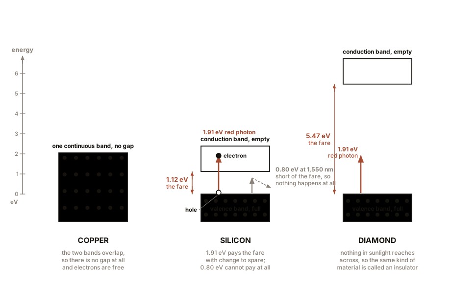
Between them is the gap, and the width of that gap, measured in electron volts, is the single most important number about any semiconductor. For silicon it is 1.12 eV at room temperature.
That number should look familiar. It is the last row of Chapter 4’s table, and now you can see what it means: 1.12 eV is the price of a ticket out of the valence band. A photon arriving with 1.91 eV, a red one, pays the fare with change to spare. A photon arriving with 0.80 eV cannot pay at all, so it does not get an electron across, and there is no such thing as paying most of the fare.
This is what makes materials sort themselves into three families.
| Material | Band gap | Behaviour |
|---|---|---|
| Copper | none; bands overlap | conductor |
| Germanium | 0.67 eV | semiconductor, easily excited |
| Silicon | 1.12 eV | semiconductor |
| Gallium arsenide | 1.42 eV | semiconductor |
| Cadmium telluride | 1.50 eV | semiconductor |
| Diamond | 5.47 eV | insulator |
| Quartz glass | about 9 eV | insulator |
There is no separate category called “insulator”. An insulator is a semiconductor whose gap is too wide for anything in ordinary life to jump it. Diamond is a semiconductor and everybody who works with it knows so; the gap is simply 5.47 eV, and neither room-temperature heat nor visible light can supply that.
Section 3: Pure Silicon Is Nearly Useless
Now measure what pure silicon actually does, and it is discouraging.
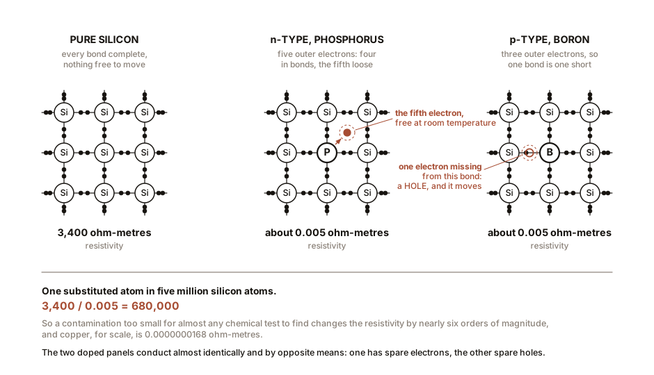
At room temperature the thermal jostling frees only about ten billion electrons per cubic centimetre out of the five hundred billion billion silicon atoms sitting there. That is one atom in five thousand million million contributing a carrier.
The result is a resistivity of roughly 3,400 Ω·m for pure silicon, against 0.0000000168 Ω·m for copper. Copper conducts about two hundred thousand million times better.
So pure silicon is not a useful conductor, and a solar cell made of pure silicon would generate its electrons and then fail to get them anywhere. What fixes this is the trick that built the entire electronics industry.
Section 4: Doping, and What It Actually Does
Silicon has four outer electrons per atom and uses all four in bonds. Its neighbours in the periodic table do not.
Phosphorus has five. Put a phosphorus atom into the silicon lattice where a silicon atom would have been. Four of its electrons go into the four bonds the site requires. The fifth has no bond to join. It sits there loosely attached, needing only about 0.045 eV to break away completely, which room-temperature heat supplies easily.
So every phosphorus atom donates one free electron, and it does it at any temperature you would care to live at. Silicon doped this way is n-type, for negative, because the mobile carriers are electrons.
Boron has three. Put a boron atom in a silicon site. It has three electrons for four bonds, so one bond is left one electron short. That deficiency is a hole, and a neighbouring valence electron can hop into it, leaving a hole where it came from. The hole moves. It behaves in every respect like a positive particle drifting through the crystal, and it is entirely legitimate to treat it as one.
Silicon doped with boron is p-type, for positive.
Now the arithmetic that makes this astonishing. A typical solar cell base is doped at about ten thousand million million boron atoms per cubic centimetre. Silicon has fifty thousand million million million atoms per cubic centimetre. The ratio is one dopant atom for every five million silicon atoms.
That amount of contamination, which would be undetectable by almost any chemical means, drops the resistivity from 3,400 Ω·m to about 0.005 Ω·m.
3,400 / 0.005 = 680,000
A factor of nearly seven hundred thousand, from one part in five million. That is the sentence to carry out of this chapter. It is also why the semiconductor industry is obsessive to the point of absurdity about purity: if one part in five million changes the material’s behaviour by six orders of magnitude, then an unintended part in five million does the same thing, unpredictably, and your wafer is scrap.
ON THE BENCH: Watch a diode’s forward voltage give away its band gap
Parts: one silicon diode such as a 1N4148, pennies; one germanium diode such as a 1N34A, about $1; one white LED, pennies; a 9 V battery; a 1 kΩ resistor; a multimeter. Cost: under $5. Time: 20 minutes. Hazards: none. Method: wire battery, resistor and diode in series, the right way round so current flows. Measure the voltage across the diode alone, not across the whole loop. Repeat for each part. What you should see: germanium about 0.3 V, silicon about 0.7 V, a white LED about 3.0 V. Now compare that to the band gaps: germanium 0.67 eV, silicon 1.12 eV, and the gallium nitride in a white LED about 3.4 eV. The order is identical and the numbers track. The voltage it takes to push current through a junction is set by the same energy gap that decides which photons a cell can convert, because it is the same gap. One measurement, taken with a battery and a resistor in twenty minutes, and you have the band gaps of three materials in the right order. If germanium reads high: you may have a Schottky diode, which reads around 0.3 V for a different reason. Check the part number.
Section 5: What the Two Types Are For
n-type silicon has spare electrons. p-type silicon has spare holes. Separately, each is simply a mediocre conductor with a peculiar temperature habit, and neither one generates anything.
Put them in contact and something new happens, and it is the something that Chapter 6 is entirely about. What follows here is the setup, not the payoff.
The free electrons on the n side are wandering. The holes on the p side are wandering. At the boundary, electrons stray across into p-type territory, find holes, and drop into them. Holes stray the other way and are filled. Both carriers vanish from a thin region either side of the boundary.
That leaves a zone with no mobile carriers in it at all, and, crucially, with the fixed dopant atoms now electrically unbalanced: phosphorus atoms on the n side that have lost their spare electrons are positively charged, and boron atoms on the p side that have gained one are negatively charged.
Fixed positive charge on one side, fixed negative charge on the other, and nothing mobile between them. That is an electric field, built into the crystal, with no battery anywhere.
SLOW DOWN. Check Your Understanding: The thermistor at the start of this chapter showed that a semiconductor conducts better when it is hot, because heat frees more carriers. A solar panel, as Chapter 1 hinted and Chapter 9 will prove, produces less power when it is hot. Those two facts appear to contradict each other. They do not. Work out how both can be true before reading on.
The resolution is that a solar cell’s problem is never a shortage of carriers. Sunlight supplies them by the sextillion, far more than heat ever will. What a cell needs is voltage, and voltage is what heat destroys.
Think about what the built-in field of Section 5 depends on. It exists because one side has a surplus of electrons and the other does not. Heat generates electron-and-hole pairs everywhere, indiscriminately, on both sides. Those thermally generated carriers do not care which side of the junction they are on, so they blur the very distinction the field depends on. Heat makes the two sides of the junction more alike, and the voltage across a junction is a measure of how unlike they are.
So: heat raises the current a semiconductor will pass, which is the thermistor. Heat lowers the voltage a junction can hold, which is the panel. Both are the same mechanism seen from two ends, and a solar cell is a device that cares far more about the second. Keep that, because it is the reason cold bright days are the best days, and Chapter 9 will put a number on every part of it.
Chapter 6 puts the two types of silicon in contact and works out why a photon arriving in that built-in field produces a current in an external wire.

Bench Degree
Get the degree without the diploma.
Learn the material, not how to pass the exam.